Acousto-Electric Conversion
To analyze the sound digitally, we must first convert the acoustic sound waves into an electrical signal using a microphone. To do this, a JLI 2555 electret condenser capsule will be used as our transducer.
TipCapacitor and Condenser tidbit
Fun fact, the words Capacitor and Condenser are historically the same word, with condenser being the original term. Originally they thought that electricity was a fluid, and that charges would “condense” on the plates.
While English speakers (especially in the US) standardized on the word Capacitor in the mid-20th century, most of the world stuck with the original terminology derived from Volta’s “Condenser.”
- 🇩🇪 German: Kondensator
- 🇯🇵 Japanese: Kondensa (コンデンサ)
- 🇪🇸 Spanish: Condensador
- 🇫🇷 French: Condensateur
- 🇷🇺 Russian: Kondensator (Конденсатор)
- 🇵🇱 Polish: Kondensator
The Condenser Transducer
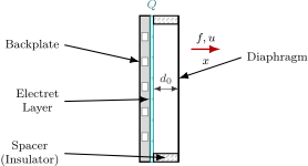
The JLI-2555 acts as a variable capacitor designed to detect acoustic pressure changes. The capsule consists of a parallel-plate capacitor structure with four critical components:
- The Backplate: A stationary metal disc perforated with holes to allow for air damping (controlling a mechanical Q-factor). In this “back-electret” design, the backplate is fused with a thin layer of electret material (typically a fluoropolymer).
- The Electret Layer: This material has been subjected to a massive electrostatic field during a heating/cooling cycle in manufacturing. This process aligns internal dipoles, effectively “freezing” a permanent static charge (Q) onto the backplate.
- The Diaphragm: A movable, low-mass Mylar film (approx. 3–6 \mu m thick) sputtered with gold to make it conductive. It is tensioned directly above the backplate.
- The Spacer: A microscopic insulating ring that maintains a specific resting air gap, d_0 (typically 20\mu m - 50\mu m), between the diaphragm and the backplate.
The frozen charge in the electret layer creates a constant electrostatic field E across the air gap without requiring an external polarizing voltage (unlike “True Condenser” microphones which typically require a DC voltage to polarize the plates).
Governing Equations ■
To model the conversion of mechanical energy to electrical energy, we rely on the capacitance, and its relationship to charge, voltage, and displacement.
Capacitance Definition
The capacitance C of a parallel plate sensor is defined by geometry:
C(t) = \frac{\epsilon A}{d(t)}
Where:
- \epsilon: is the permittivity of the dielectric material between the plates (usually air, so \epsilon \approx \epsilon_0, permittivity of free space).
- A: is the effective surface area of the plates (the diaphragm and the backplate).
- d(t): is the instantaneous distance between the plates, which varies with time (sound).
The Charge Equation
The relationship between Charge (Q), Capacitance (C), and Voltage (V) is:
V(t) = \frac{Q}{C(t)}
- Q is Constant: Because the electret material permanently traps the charge carriers, Q cannot change quickly.
- C(t) is Variable: As sound moves the diaphragm, C changes.
- V(t) is the Result: To satisfy the equation V = Q/C, if C changes, V must change. This fluctuating voltage is the audio signal.
Voltage Signal Transfer Function ■
We want to find the relationship between the acoustic displacement (\Delta x) and the output voltage (\Delta v). Thus we will derive the small-signal1 transfer function for the voltage signal.
1 Small-signal is a term used to describe a small change in the input signal. It is used to linearize the system and make it easier to analyze. Though passive components like capacitors and inductors are considered linear, any component outside of its operating specifications may deviate from linearity.
TipDerivation
Let the instantaneous distance d(t) be defined as the resting gap d_0 minus the acoustic displacement x(t) (where positive x indicates inward movement):
d(t) = d_0 - x(t)
Substitute the definition of d(t) into the capacitance equation, and then into the voltage equation:
V(t) = \frac{Q}{ \left( \frac{\epsilon_0 A}{d_0 - x(t)} \right) }
Rearranging terms:
V(t) = \frac{Q (d_0 - x(t))}{\epsilon_0 A}
Expanding the numerator:
V(t) = \frac{Q d_0}{\epsilon_0 A} - \frac{Q}{\epsilon_0 A} x(t)
The resulting equation reveals the signal composition:
- DC Bias Term: \frac{Q d_0}{\epsilon_0 A}. This represents the static DC voltage present across the plates due to the electret charge2.
- AC Signal Term: -\frac{Q}{\epsilon_0 A} x(t). This is the audio signal.
2 This DC voltage does not affect the audio signal, as it is typically blocked by coupling capacitors in the preamp stage of a microphone amplifier.
Note the linearity: V(t) \propto x(t). Unlike strictly non-linear transducers, the condenser microphone (for small displacements x \ll d_0) is inherently linear, resulting in very low Total Harmonic Distortion (THD).
The Need for an impedance converter
WarningRevision Needed
Add image of generic impedance converter circuit diagram
We have established that the JLI-2555 generates a linear voltage signal V(t) proportional to acoustic pressure. However, generating voltage is only half the battle; delivering that voltage to a load is our primary challenge.
The Impedance Mismatch
The capsule is fundamentally a capacitor, let us assume it has a capacitance of C_{mic} \approx 35 \text{pF}3. Its source impedance is purely reactive:
3 35 \text{pF} is a conservative “worst case” estimate. This is a typical value for a condenser microphone capsule. Nothing is ideal and the actual capacitance will vary depending on the frequency of operation and the design of the capsule. Though most will be in the range of 35 \text{pF} - 45 \text{pF} based off the consensus measurements of the TSB-2555 family (The JLI-2555 is a rebrand of the TSB-2555).
Z_{source} = \frac{1}{j \omega C_{mic}} = \frac{1}{j 2\pi f C_{mic}}
At a low audio frequency of 50 \text{Hz}:
|Z_{source}| = \frac{1}{2\pi (50)(35 \times 10^{-12})} \approx 91 \text{ M}\Omega
We have a massive source impedance. If we connect this directly to a any ordinary low impedance preamplifier like a standard microphone preamp, (Z_{load} \approx 2\text{k}\Omega), we form a voltage divider that destroys the signal:
V_{out} = V_{gen} \cdot \frac{Z_{load}}{Z_{source} + Z_{load}} \approx V_{gen} \cdot \frac{2\text{k}\Omega}{91\text{M}\Omega} \approx 0
Converter Requirements
To successfully interface this capsule, we require an active circuit stage—an Impedance Converter—that satisfies three specific conditions:
- Ultra-High Input Impedance: To prevent loading the capsule and losing low-frequency information (high-pass filtering), the input impedance must be at least 10\times the source impedance at the lowest frequency of interest. For full bandwidth, we target Z_{in} > 500 \text{ M}\Omega.
- Unity (or greater) Voltage Gain: We do not strictly need voltage amplification at this stage, but we must preserve the voltage level (A_v \approx 1).
- Low Output Impedance: The stage must be able to drive the capacitance of a microphone cable and the low input resistance of the preamp.
Device Selection: JFET vs. Op-Amp
There are two primary ways to implement this buffer:
1. Discrete Junction Field Effect Transistor (JFET)
This is the traditional method used in almost all electret microphones.
- Mechanism: The Gate of a JFET is a reverse-biased PN junction. Unlike a Bipolar Junction Transistor (BJT) which requires base current to operate (I_b = I_c / \beta), a JFET is a voltage-controlled device.
- Leakage: The gate current (I_{GSS}) is typically in the range of picoamperes (10^{-12} A), presenting an input resistance in the tera-ohm range (10^{12} \Omega).
- Topology: A Common Source or Source Follower topology converts the high-impedance voltage at the Gate into a current drive at the Source/Drain.
2. JFET-Input Operational Amplifier
In modern high-performance designs (like the “Alice” circuit), one might use an Op-Amp.
- Constraint: We cannot use a standard Bipolar Op-Amp (e.g., NE5532) because its input bias current is too high and it would drain the capsule charge.
- Solution: We can use an Op-Amp with a JFET Input Stage (e.g., OPA1642, OPA134). These integrated circuits have JFETs built into their differential input pair, offering the same high impedance benefits as a discrete JFET but with better linearity and easier gain configuration.
WarningRevision Needed
Add Image of JFET common source amplifier vs Op-Amp buffer circuit diagram
The Role of the Gigohm Bias Resistor
Whether using a discrete JFET or an Op-Amp, you will almost always see a resistor of extremely high value (1 \text{ G}\Omega to 5 \text{ G}\Omega) placed from the Gate (or Non-inverting Input) to Ground.
This component is critical for two reasons:
1. DC Stability & Bias Current Management
The primary function of R_{bias} is to prevent the amplifier from drifting into saturation.
The “Floating Node” Problem: While JFETs and JFET-input Op-Amps are often modeled as having infinite input impedance, they physically possess a non-zero Input Bias Current (I_B) or Gate Leakage Current (I_{GSS}). This is typically in the range of 2 \text{ pA} to 10 \text{ pA}.
If the microphone capsule (C_{mic}) acts as a DC open circuit and R_{bias} is omitted, the amplifier input becomes a floating node. The amplifier’s input stage will source or sink I_B into the capacitor C_{mic}, effectively turning the circuit into an integrator:
V_{in}(t) = V_{initial} + \frac{1}{C_{mic}} \int I_B \, dt
Given a constant I_B, the input voltage ramps linearly:
\frac{dV}{dt} = \frac{I_B}{C_{mic}}
Failure Mode: With I_B = 10 \text{ pA} and C_{mic} = 35 \text{ pF}, the voltage drifts at \approx 0.3 \text{ V/s}. Within seconds, the input voltage exceeds the supply rails or the Common Mode Voltage Range. The amplifier saturates (“latches”), and the audio signal is completely blocked.
The Solution: The Gigohm resistor provides a DC return path for I_B. Instead of charging the capacitor, the current flows through R_{bias}, establishing a stable, fixed DC offset:
V_{offset} = I_B \cdot R_{bias}
Using R_{bias} = 1 \text{ G}\Omega: V_{offset} = (10 \times 10^{-12} \text{ A})(1 \times 10^9 \Omega) = 10 \text{ mV}
This negligible offset keeps the amplifier biased correctly in its linear region.
2. Defining the High-Pass Filter (HPF) Corner
The second function of R_{bias} is to preserve low-frequency bandwidth.
The source capacitance C_{mic} and the input resistance R_{bias} form a first-order RC High-Pass Filter. The cutoff frequency (f_c, -3dB point) is governed by:
f_c = \frac{1}{2\pi R_{bias} C_{mic}}
Why 1 Gigohm? If we used a standard resistor value, such as 1 \text{ M}\Omega, with our 35 \text{ pF} capsule, the bass response would be destroyed:
f_c = \frac{1}{2\pi (1 \times 10^6)(35 \times 10^{-12})} \approx 4,547 \text{ Hz}
This would result in a “tinny” sound with no frequencies below the upper-midrange. By selecting 1 \text{ G}\Omega:
f_c = \frac{1}{2\pi (1 \times 10^9)(35 \times 10^{-12})} \approx 4.5 \text{ Hz}
This ensures the full audible spectrum (20 \text{ Hz} - 20 \text{ kHz}) is passed to the preamp without attenuation or phase shift.
Alternative Transducer Impedance Needs
It is important to note that the high-impedance JFET converter discussed above is specific to Capacitive Transducers (Condenser/Electret microphones). Different transducer families obey different physical laws and therefore require different interface circuits.
Dynamic and Ribbon Microphones
These are Inductive Transducers. They generate voltage by moving a conductor through a magnetic field (V = B \cdot l \cdot v). - Source Impedance: Low and resistive (typically 150 \Omega - 300 \Omega). - Converter Needs: They do not require a JFET buffer. They can drive a standard preamplifier input (2 \text{ k}\Omega) directly because Z_{source} \ll Z_{load}. In fact, placing a high-impedance buffer in front of a dynamic mic typically raises the noise floor without improving signal transfer.
Piezoelectric Contact Mics
Like condensers, these are capacitive and high-impedance, often requiring buffers similar to the JFET circuit, though usually with even higher input impedance requirements (> 10 \text{ M}\Omega) to preserve bass response.
All this to say, the JFET buffer is not a universal “microphone fixer”; it is a specific solution to the high-reactance problem inherent to the equation V = Q/C.
The Need for a Pre-amplifier ■
Once the signal leaves the impedance converter, it has sufficient current drive to travel down a cable, but it is still electrically fragile. To be useful in a digital system, it must be processed by a Pre-Amplifier.
Signal Levels and Voltage Gain
The output of the JLI-2555 (buffered) is at Mic Level.
- Mic Level: typically 2 \text{ mV} to 10 \text{ mV} RMS (approx -60 dBV to -40 dBV).
- Line Level (Consumer): -10 \text{ dBV} (\approx 316 \text{ mV}).
- Line Level (Pro): +4 \text{ dBu} (\approx 1.23 \text{ V}). -ADC Input Requirement: A typical Analog-to-Digital Converter (ADC) expects a signal that swings close to its reference voltage (often 2 \text{ V}_{pp} to 5 \text{ V}_{pp}) to maximize bit-depth resolution.
If we feed the raw 8mV capsule signal directly into a 2V ADC, we utilize less than 1% of the available dynamic range. The result would be digital audio with extremely poor Signal-to-Noise Ratio (SNR) and severe quantization noise.
The Pre-Amp’s Job: The pre-amplifier must provide linear voltage gain (A_v) to bridge this gap: Gain_{dB} = 20 \log \left( \frac{V_{target}}{V_{mic}} \right) To boost 8 \text{ mV} to 1.2 \text{ V}, we need roughly +44 dB of clean gain.
Practical Standards vs. Physical Reality
In professional audio, we rely on standards like Balanced XLR connections and dedicated Mic-In ports.
- Balanced Audio: Uses Differential Mode Rejection (Pin 2 Hot, Pin 3 Cold) to cancel out electromagnetic interference (RFI/EMI) picked up by long cable runs.
- Mic-In Ports: Provide the necessary gain stages and often DC phantom power.
WarningRevision Needed
Add animaition of Differential Mode Rejection
However, from a fundamental EE perspective, these standards are practical solutions to environmental noise, not strict requirements for signal digitization.
The Fundamental Truth: If an audio signal—regardless of whether it comes from a mic, a guitar, or a synth—is amplified to the correct peak-to-peak voltage and transmitted without interference, it can be read by any ADC.
- You could wire the JLI-2555 directly to a laboratory oscilloscope or a bare ADC chip on a breadboard, provided the voltage levels match.
- The computer does not “know” if a signal came from an XLR cable or a breadboard wire; it only reads the voltage present at the analog to digital converter.
Therefore, the signal chain is strictly defined by Impedance Matching (Stage 1) and Voltage Scaling (Stage 2), rather than the shape of the physical connector.
Conclusion
For a practical example of how a a microphone circuit could be implemented