This documentation is essentially complete; a PCB render and build photos are still to come. Corrections and edit requests are welcome — submit one at the margin of the page or contact the team.
Building a purely analog microphone is surprisingly simple in theory, with only a few complexities in practice. Thus, for the Piano Acoustics & Tuning Report, a basic proof of concept microphone circuit has been created using a JLI-2555. All circuit and PCB Files can be found here.
WarningDisclaimer
This circuit is not intended for professional use. It is a basic proof of concept and is not designed to be used in a production environment. It is intended to be a fun, reproducible project to learn about microphones and audio circuits that many can replicate at home without any dedicated audio equipment (such as audio interfaces or preamps).
That being said, the circuit was designed to have an incredibly low noise floor while using as few components as possible. This circuit can be edited by anyone. The power supply can be easily modified, and the way the output signal is delivered can be changed to suit the needs of the user.
That being said… if you are looking for a cheap, professional microphone circuit that can run off of phantom power, you should probably look at something like the iconic OPA Alice Circuit. You can build it for yourself or order it pre-built someplace like here.
Design Constraints
To make this circuit as reproducible and accessible to even novice electronics enthusiasts as much as possible, the following constraints were imposed
NoteList of Constraints
All components must be through hole and non-obsolete.
Surface mount soldering is not accessible to everyone. Therefore all components must be through hole.
Many “classic” components are no longer in production. They are either being discontinued or being replaced by their surface mount counterparts. This is a pain for hobbyists, who may have difficulty sourcing a part or unknowingly buy counterfeit components, not knowing that these components are no longer in production.
There should be no need for dedicated audio equipment. Many people starting out to learn will likely be young and have little to no disposable income, fact. This means that the design should not rely on expensive equipment to function such as audio interfaces or preamps.
The design should be as simple as possible. The fewer components the better. The fewer steps the better. The fewer mistakes the better. The lower the cost the better.
Our last constraint is that of the actual analog to digital conversion. For simplicity, we want to use a simple USB type-C ADC, while also maximizing the quality of the signal. Therefore we want to use a 24-bit ADC. The only readily available Type-C, 24-bit ADC found at the time of writing was a generic USB-C adapter exposing both a line-in and a mic-in input.
WarningNote on non-obsolete components
In the coming future, just about all through hole Op Amps will be no longer in production. These components, much like JFETs, are being replaced by their surface mount counterparts. Major manufacturers like TI and Analog Devices have no need to manufacture through hole components anymore, since hobbyists are not their target market.
There are “boutique” manufacturers that sell through hole components that are no longer in production (such as Linear Integrated Systems). These components are often more expensive since they are not produced in the scale of the major manufacturers but they do provide a reliable source of these well sought after devices.
Another approach to solving this “issue” is to use a surface mount to through-hole adapter. This obviously still requires surface mount soldering but there are websites that sell these smd components pre-soldered to through-hole adapters for a reasonable price.
To simplify our design, we will rely on using a line-level signal. This is done to avoid the need for a differential amplifier to deal with the noise interference that would normally come from using an unbalanced mic input.
Why Line-Level Signals are Less Susceptible to Noise
The primary difference between a mic-level signal and a line-level signal is voltage magnitude. A raw mic-level signal is very weak (often a few millivolts). As this weak signal travels down a wire, it picks up electromagnetic interference (hum, RFI). When the signal is eventually amplified, that noise is amplified along with it.
Code
import numpy as npimport plotly.graph_objects as go# 1. Setup Time Domain in Seconds (for accurate frequency math)t = np.linspace(0, 0.005, 1000)tt = t *1000# Millisecond array for the x-axis# 2. Define the Mic-Level Signal (~11.17 mV peak)mic_signal =11.17* np.sin(2* np.pi *1000* t) # 3. Define the EMI/RFI Noisenoise = (2.0* np.sin(2* np.pi *60* t) +1.0* np.sin(2* np.pi *50000* t) + np.random.normal(0, 0.5, len(t)))# 4. Combine Signal and Noisemic_with_noise = mic_signal + noise# 5. Build the Plotly Figureplot = go.Figure()plot.add_trace(go.Scatter(x=tt, y=mic_signal, mode='lines', name='Pure Mic Signal (~11.2mV Peak)', line=dict(color='blue', dash='dash')))plot.add_trace(go.Scatter(x=tt, y=mic_with_noise, mode='lines', name='Mic Signal + EMI/RFI', line=dict(color='red')))plot.add_trace(go.Scatter(x=tt, y=noise, mode='lines', name='Standalone Noise Floor', line=dict(color='gray', width=1)))# 6. Formatting Base Layoutplot.update_layout( title="Mic-Level Signal Susceptibility to EMI/RFI", xaxis_title="Time (ms)", yaxis_title="Amplitude (mV)", legend=dict(x=0.99, y=0.01, xanchor='right', yanchor='bottom', bgcolor='rgba(128, 128, 128, 0.2)'), margin=dict(l=40, r=40, t=40, b=40))# 7. Render Light Versionplot.update_layout(template="plotly_white")display(plot)# 8. Render Dark Versionplot.update_layout(template="plotly_dark")display(plot)
By amplifying the signal to “Line Level” (hundreds of millivolts or more), the Signal-to-Noise Ratio of the desirable signal to the external cable noise becomes much higher. The signal is effectively “loud” enough to drown out the interference picked up by the cable.
Code
import numpy as npimport plotly.graph_objects as go# 1. Setup Time Domain in Secondst = np.linspace(0, 0.005, 1000)tt = t *1000# 2. Define the Line-Level Signalline_signal =452.5* np.sin(2* np.pi *1000* t)# 3. Define the EMI/RFI Noise (Identical to mic-level example)noise = (2.0* np.sin(2* np.pi *60* t) +1.0* np.sin(2* np.pi *50000* t) + np.random.normal(0, 0.5, len(t)))# 4. Combine Signal and Noiseline_with_noise = line_signal + noise# 5. Build the Plotly Figureplot = go.Figure()plot.add_trace(go.Scatter(x=tt, y=line_signal, mode='lines', name='Pure Line Signal (~452mV Peak)', line=dict(color='blue', dash='dash')))plot.add_trace(go.Scatter(x=tt, y=line_with_noise, mode='lines', name='Line Signal + EMI/RFI', line=dict(color='green', width=2)))plot.add_trace(go.Scatter(x=tt, y=noise, mode='lines', name='Standalone Noise Floor', line=dict(color='gray', width=1)))# 6. Formatting Base Layoutplot.update_layout( title="Line-Level Signal Overcoming EMI/RFI", xaxis_title="Time (ms)", yaxis_title="Amplitude (mV)", legend=dict(x=0.99, y=0.01, xanchor='right', yanchor='bottom', bgcolor='rgba(128, 128, 128, 0.2)'), margin=dict(l=40, r=40, t=40, b=40))# 7. Render Light and Dark Versionsplot.update_layout(template="plotly_white")display(plot)# 8. Render Dark Versionplot.update_layout(template="plotly_dark")display(plot)
SNR comparison:
To calculate SNR, we first need to determine the total RMS (Root Mean Square) voltage of the simulated interference. Our noise profile consists of three components: - 60Hz Mains Hum: 2.0 mV peak \approx 1.41 mV RMS - 50kHz RFI: 1.0 mV peak \approx 0.71 mV RMS - Random Ambient/Thermal Noise: \approx 0.50 mV RMS
When combined, the total effective noise floor is approximately 1.66 mV RMS. The standard formula for calculating voltage SNR in decibels is:
Analysis: An SNR of 13.5 dB is extremely poor for audio. The desirable audio signal is barely louder than the interference. This is why the red line in the first plot looks heavily distorted; the noise is actively competing with the primary waveform. If this weak signal were to travel down a cable and be amplified later, the noise would be amplified right alongside it.
Line-Level SNR
The circuit uses an OPA134 op-amp to apply a gain of 40 (approximately 32 dB), boosting the raw signal to a healthy 320 mV RMS line-level signal right at the source.
Analysis: By amplifying the signal inside the microphone, the ratio of the desirable signal to the external cable noise becomes vastly higher. The noise floor remains exactly the same (1.66 mV), but because the signal is now 320 mV, the noise becomes mathematically and audibly insignificant. The signal is effectively “loud” enough to completely drown out the interference. The difference between the two ratios is exactly 32 dB, which perfectly mirrors the 32 dB of gain provided by the pre-amplifier stage.
Circuit Design
JLI-2555 Schematic
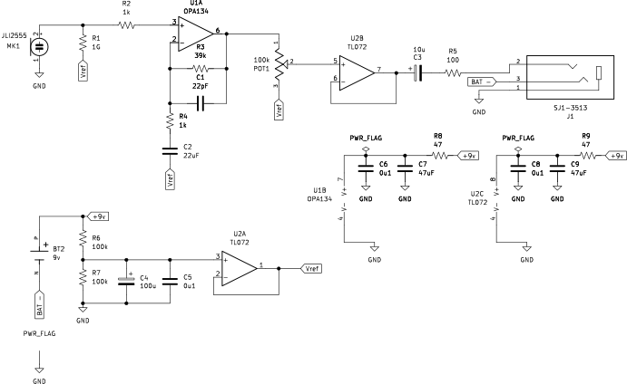
A unipolar power supply1 is used. For simplicity, a 9V battery is used. Thus the signal must be centered around ~4.5 volts, about half of that of the supply voltage.
1 A unipolar power supply is a power supply that provides a single voltage level. It is the opposite of a bipolar power supply, which provides a positive and negative voltage level.
The Impedance Converter
Impedance Buffer Schematic
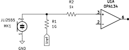
The JLI-2555 used here is a “FET-less” electret capsule. This means it is a raw capacitive sensor without the internal JFET usually found in electret microphones. Because of this, the output impedance of the capsule is incredibly high (capacitive), requiring an interface with extremely high input impedance to preserve the low-end frequency response.
We interface the capsule directly to the OPA134 op-amp (U1A). The input is biased to our reference voltage (Vref) through a massive 1 Gigaohm resistor (R1).
Why use the Non-Inverting Topology?
We chose the non-inverting topology for U1A primarily for Input Impedance. In an inverting topology, the input impedance is determined largely by the input resistor. To sit far above the source impedance of the capsule, that input resistor would need to be huge, and the feedback resistor would need to be even larger to achieve gain, which is impractical.
In the non-inverting configuration, the input impedance is determined by the op-amp’s inherent input impedance (which is extremely high for the FET-input OPA134) in parallel with our bias resistor R1 (1GΩ). This ensures we do not “load down” the capsule, preserving the signal integrity.
Biasing to Half-Supply (Vref)
Since we are using a single 9V battery (0V and 9V), the op-amp cannot handle negative voltages relative to ground. Audio is an AC signal that swings positive and negative. By biasing the input to 4.5V (Vref) via R1, we create a “Virtual Ground.” The audio signal now swings up to ~6V and down to ~3V, keeping it safely within the power rails of the op-amp.
The Input Capacitance and R2
The OPA134’s JFET input stage is not an ideal open circuit. Its datasheet gives 10^{13}\ \Omega \parallel 8\ \text{pF} differential and 10^{13}\ \Omega \parallel 6\ \text{pF} common-mode — the same order of magnitude as our ~35 pF capsule, so it does two things.
It forms a capacitive divider with the capsule, C_{mic}/(C_{mic} + C_{in}), costing about -1.8 dB before any gain. Board stray capacitance adds to C_{in}, so the trace from the capsule to U1A is kept short.
It also gives R2 its purpose. In series with C_{in}, it forms a low-pass:
Far above audio, so R2 is transparent to the signal while rolling off RF before it reaches the input.
NoteA known trade-off of driving the capsule directly
Section 6.2.3 of the OPA134 datasheet notes that its p-channel JFET input capacitance varies with common-mode voltage, causing increased distortion in non-inverting configurations when source impedances above 2 kΩ are left unmatched between the inputs.
A JFET gate is a reverse-biased junction, so its depletion capacitance tracks the voltage across it. In a non-inverting stage the input follows the signal, making that capacitance signal-dependent and therefore nonlinear; in an inverting stage the input sits at virtual ground and the effect disappears. U1A is non-inverting with a source impedance far above 2 kΩ, so the circuit accepts this in exchange for simplicity.
This has not been measured on the built circuit — it is derived from the datasheet, not bench data. For measurements across many op-amps, see Samuel Groner’s Operational Amplifier Distortion.
The Pre-Amplifier
Pre-Amplifier Schematic
Typically one would utilize a separate pre-amplifier stage to amplify the signal to a level that is compatible with the ADC. Typical JFET buffers are designed to be unity gain buffers2.
2 Why are they unity gain buffers? There are two main configurations for a JFET amplifier. The first is the common source configuration, and the second is the common drain configuration. The common source configuration allows for voltage amplification however may result in amplifying noise and a higher than desired output impedance. The common drain configuration is a voltage follower and does not amplify the signal and thus also the noise. However, it has a much lower output impedance than the common source configuration.
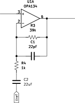
In our case, because we are using a OPA134, we can follow typical op amp design practices to amplify the signal directly at the source.
Sensitivity and Gain Calculation
To determine the required gain, we first calculate the voltage the JLI capsule outputs at standard speaking volume.
The JLI-2555 is rated at -42 dBV/Pa.
Reference: 1 Pascal (94 dB SPL).
Output:10^{(-42/20)} \approx 7.9 \text{ mV RMS}.
This confirms that for a standard speaking volume at 1 meter, the capsule generates a raw AC signal of approximately 8mV sitting on top of the internal DC bias. To bring this up to a standard “Line Level” (consumer line level is often -10dBV, or ~316mV RMS), we need significant gain.
We set the gain of the OPA134 (U1A) using resistors R3 (39kΩ) and R4 (1kΩ). The gain formula for a non-inverting amplifier is:
A gain of 40 (approx 32dB) boosts our 8mV signal to 320mV, which is a healthy line-level signal perfect for the ADC input.
The Power Supply
Power Supply Schematic
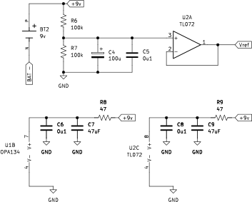
To maintain a clean signal, the power supply must be stable. We generate our 4.5V reference voltage (Vref) using a voltage divider (R6, R7) buffered by a TL072 op-amp (U2A). This “Active Virtual Ground” is far superior to a simple resistor divider, as it can source and sink current without the voltage sagging.
Noise Rejection: The design offers excellent noise rejection for three reasons:
Buffered Reference: The reference voltage is heavily filtered by C4 (100\muF) before entering the buffer. The cutoff frequency of this filter is approx 0.03Hz. This means even if the 9V battery sags under load, Vref remains rock-steady.
Rail Filtering: Each op-amp power pin is fed through an RC Low-Pass filter (e.g., R8/C7). This prevents high-frequency oscillation and RF interference from entering the op-amps via the power rails.
Intrinsic PSRR: The OPA134 has a Power Supply Rejection Ratio (PSRR) of roughly 100dB. Combined with the external filters, power supply noise is effectively non-existent.
The Output Stage
Output Stage Schematic
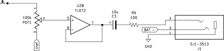
Finally, the signal passes through a Volume Potentiometer (POT1), allowing the user to attenuate the signal if the source is too loud. This is followed by a unity-gain buffer using the second half of the TL072 (U2B). This buffer isolates the volume pot from the outside world, ensuring the output impedance remains low and constant.
The signal exits through a TS (Tip-Sleeve) Jack (J1). A 10uF capacitor (C3) blocks the 4.5V DC offset, allowing only the AC audio to pass.
Power Switching: Cleverly, the Ring connection of the output jack is used as a power switch. When a Mono (TS) cable is inserted, the Sleeve shorts the Ring to Ground, completing the battery circuit.
Noise Analysis
The circuit is designed for extremely low noise. The analysis is broken down into two main stages.
1. Input & Pre-Amplifier Stage (U1A)
The input impedance conversion and voltage amplification happen in a single stage using the OPA134.
R1 (1G\Omega) - The Bias Resistor: Ideally, a 1G\Omega resistor generates massive thermal noise (\approx 4 \mu V/\sqrt{Hz}). However, the microphone capsule (~35 pF) shunts it away: R1’s own noise drives through the resistor and out through the capacitor, a low-pass\frac{1}{1 + j\omega R_1 C_{mic}} cornering near 4.5 Hz. The same network is a high-pass for the signal, which arrives through the capacitor instead — derived here.
R2 (1k\Omega) - The RF Stopper: The noise density of this resistor is roughly 4 \text{ nV}/\sqrt{Hz}. This is negligible compared to the intrinsic noise floor of the room. Its RF-stopping role is covered in The Impedance Converter.
Op-Amp Noise (OPA134): The OPA134 is a premium audio op-amp with an ultra-low noise floor of 8 nV/\sqrt{Hz} at 1kHz. Because it is a FET-input op-amp, it also has incredibly low current noise, which is critical when dealing with high-impedance sources like the JLI-2555.
Summary: The dominant noise source in this stage is not the electronics, but the JLI-2555 capsule itself (self-noise) and the acoustic noise of the room.
2. Output Buffer Stage (U2B)
The signal enters the TL072 buffer stage after passing through the volume potentiometer.
TL072 Noise: The TL072 is slightly noisier than the OPA134 (\approx 18 \text{ nV}/\sqrt{Hz}). However, by the time the signal reaches this stage, it has already been amplified by 40x (32dB).
Signal-to-Noise Ratio (SNR): With the signal already at 320 mV, a noise density of 18 \text{ nV}/\sqrt{Hz} added at this stage is mathematically insignificant. The noise floor is set by the first stage; the second stage simply passes it along.
PCB Design
The board was laid out in KiCad as a two-layer, 80 mm × 70 mm through-hole design. The full project files (schematic, layout, and footprint libraries) are in the project repository.
Continuous Ground Plane
The entire bottom copper layer is a single filled ground pour. Signal routing is deliberately kept on the top layer — of the 99 routed track segments, 96 sit on the front copper and only 3 on the back — so the plane beneath them remains effectively uninterrupted, with just 5 vias stitching between layers.
Every return current takes the path of least impedance, which at audio frequencies means flowing directly beneath its outgoing trace. An unbroken plane keeps that loop area small, limiting EMI/RFI pickup and keeping the high-impedance input at U1A off a shared return path. That node sits behind a 1 GΩ bias resistor, so any noise coupled into it is amplified by the full 32 dB of the pre-amp stage.
Pads connect to the pour through thermal reliefs (0.5 mm spoke width and gap) rather than solid copper, so the plane does not sink so much heat that hand-soldering the through-hole parts becomes difficult — a direct consequence of the “reproducible at home” constraint.
The Enclosure as a Shield
The tin can is not just a housing. It is bonded to circuit ground by a wire soldered directly to the can, which turns the enclosure into a grounded Faraday cage around the electronics.
This protects the same vulnerable node as the ground plane: an unshielded high-impedance input picks up mains hum and RF from the surrounding room, and grounding the can gives that interference a low-impedance path away before it reaches U1A. With the RC-filtered rails and the R2 RF stopper, this is what keeps the noise floor dominated by the capsule’s own self-noise rather than the environment.
The Audio to Digital Converter (ADC)
As mentioned in the list of constraints, we will be using a USB type-C ADC adapter — a generic 24-bit USB-C adapter exposing both a line-in and a mic-in input.